
Generating Reports for Debugging
FPGA Compiler includes additional commands that provide CLB and IOB information for debugging purposes.
Use the following commands before using the Replace FPGA command to replace CLBs and IOBs with gates.
Generating a Configuration Report
You can generate a report that gives you CLB and IOB configuration information similar to the reports generated with the Xilinx software. This report contains information cell configuration and the logic function it implements.
To generate a CLB and IOB configuration report, first generate a symbol or schematic view for the design using either of the following methods.
- From Design Analyzer Menu, select Tools
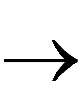 FPGA Compiler
  Report
  Cell
Cell  Apply.
- From the DC shell prompt, enter report_cell, ENTER.
The system displays the following output in the Command window.
*************************************

Report : cell

Design : count8

Version: v3.4b

Date   : Tues Dec 10 09:22:21 1996

*************************************


Attributes:

    b - black box (unknown)

    BO - reference allows boundary optimization

    h - hierarchical

    n- noncombinational

    r - removable

    u- contains unmapped logic


Cell                 Reference         Library         Area   Attributes

-------------------------------------------------------------------------

U62                  iob_4000          xfpga_4000-5    1.00    n

U64                  iob_4000          xfpga_4000-5    1.00    n

U66                  iob_4000          xfpga_4000-5    1.00    n

U68                  iob_4000          xfpga_4000-5    1.00    n

U70                  iob_4000          xfpga_4000-5    1.00    n

U72                  iob_4000          xfpga_4000-5    1.00    n

U74                  iob_4000          xfpga_4000-5    1.00    n

U76                  iob_4000          xfpga_4000-5    1.00    n

U78                  iob_4000          xfpga_4000-5    1.00    n

U80                  iob_4000          xfpga_4000-5    1.00    n

U82                  BUFG_F            xprim_4000-5    0.00    n

U83                  clb_4000          xfpga_4000-5    1.00    n

U85                  clb_4000          xfpga_4000-5    1.00    n

U87                  clb_4000          xfpga_4000-5    1.00    n

U89                  clb_4000          xfpga_4000-5    1.00    n

add_21/plus/LEFT_UNSIGNED_ARG_799

                     count8_inc_dec_ub_8_0             4.00    BO, h, n

-------------------------------------------------------------------------

Total 16 cells                                        18.00
Detailed FPGA Configuration Information:

Cell Name: U62   TYPE: IOB

       OUT:O

       PAD:FAST          I1:    I2:    TRI:


Cell Name: U64   TYPE: IOB

       OUT:O

       PAD:FAST          I1:    I2:    TRI:


Cell Name: U66   TYPE: IOB

       OUT:O

       PAD:FAST          I1:    I2:    TRI:


Cell Name: U68   TYPE: IOB

       OUT:O

       PAD:FAST          I1:    I2:    TRI:


Cell Name: U70   TYPE: IOB

       OUT:O

       PAD:FAST          I1:    I2:    TRI:


Cell Name: U72   TYPE: IOB

       OUT:O

       PAD:FAST          I1:    I2:    TRI:


Cell Name: U74   TYPE: IOB

       OUT:O

       PAD:FAST          I1:    I2:    TRI:


Cell Name: U76   TYPE: IOB

       OUT:O

       PAD:FAST          I1:    I2:    TRI:


Cell Name: U78   TYPE: IOB

       OUT:O

       PAD:FAST          I1:    I2:    TRI:


Cell Name: U80   TYPE: IOB

       OUT:O

       PAD:FAST          I1:    I2:    TRI:


Cell Name: U83   TYPE: CLB

       X:              Y:         XQ:QX      YQ:QY

       H1:             DIN:C1     SR:C2      EC:C3

       DX:DIN          DY:G       FFX:EC:RESET:K

                                              FFY:EC:RESET:K

       EQUATE G = (G1)

       FFX_NAME:QOUT_reg<1>     FFY_NAME:QOUT_reg<0>


Cell Name: U85   TYPE: IOB

       X:              Y:         XQ:QX      YQ:QY

       H1:             DIN:C1     SR:C2      EC:C3

       DX:DIN          DY:G       FFX:EC:RESET:K

                                              FFY:EC:RESET:K

       EQUATE G = (G1)

       FFX_NAME:QOUT_reg<3>     FFY_NAME:QOUT_reg<2>


Cell Name: U87   TYPE: IOB

       X:              Y:         XQ:QX      YQ:QY

       H1:             DIN:C1     SR:C2      EC:C3

       DX:DIN          DY:G       FFX:EC:RESET:K

                                              FFY:EC:RESET:K

       EQUATE G = (G1)

       FFX_NAME:QOUT_reg<5>     FFY_NAME:QOUT_reg<4>


Cell Name: U89   TYPE: IOB

       X:              Y:         XQ:QX      YQ:QY

       H1:             DIN:C1     SR:C2      EC:C3

       DX:DIN          DY:G       FFX:EC:RESET:K

                                              FFY:EC:RESET:K

       EQUATE G = (G1)

       FFX_NAME:QOUT_reg<7>     FFY_NAME:QOUT_reg<6>
Generating a Hierarchical Schematic
As an alternative to interpreting the Report Cell output listing, you can direct FPGA Compiler to replace all CLB and IOB cells with an equivalent set of logic from the target libraries. Use the generated schematic to determine what logic implemented the CLBs and IOBs.
To generate a hierarchical CLB and IOB schematic, perform the following steps.
- Save your original design as a DB file using one of the following methods. You do this because the commands used to generate the hierarchical CLB and IOB schematic alter your design's hierarchy and logical representation.
Select File  Save As
  File Format `DB' from the Design Analyzer menu then click on OK, or enter the following in the command window.
write -format db -hierarchy -output design.db
- Select Tools
 FPGA Compiler
  FPGA Cells to Gates Options from the Design Analyzer menu, or enter the following in the command window.
replace_fpga
- After you finish viewing the hierarchical schematic, read in the original DB file using one of the following methods.
Select File  Read
Read  File Format `DB' from the Design Analyzer menu, specifying the appropriate file name. Then click on OK, or enter the following in the command window.
read -format db design.db
Creating a Level for Each CLB and IOB
Create a hierarchy level for each CLB and IOB or a hierarchy level for each function generator to assist you in locating logic or signals for debugging purposes. To create a level of hierarchy, use one of the following methods.
Select Tools  FPGA Compiler
  FPGA Cells to Gates Options
  Create a Level of Hierarchy for each CLB and IOB from the Design Analyzer menu.
You can also enter the following at the DC Shell prompt.
replace_fpga -group_cells
After you select these options, the resulting logic does not accurately reflect the timing of the actual CLB and IOB implementation. Timing or area reports then produce inaccurate results.
Generating a Level for Each Function Generator
Generate hierarchical schematics that show the logic in each function generator it implements. This process replaces each CLB by an F, G, or H function generator, along with the used flip-flops. The function generators add an additional level of hierarchy. To create a level of hierarchy for each function generator, do one of the following.
Select Tools  FPGA Compiler
  FPGA Cells to Gates Options
  Create a Level of Hierarchy for each “Table-lookup” from the Design Analyzer menu.
You can also enter the following at the DC Shell prompt.
replace_fpga -group_tlus
You can now view the implementation of the function generators.

![]() FPGA Compiler
FPGA Compiler ![]() FPGA Cells to Gates Options
FPGA Cells to Gates Options ![]() Create a Level of Hierarchy for each CLB and IOB from the Design Analyzer menu.
Create a Level of Hierarchy for each CLB and IOB from the Design Analyzer menu.![]() FPGA Compiler
FPGA Compiler ![]() FPGA Cells to Gates Options
FPGA Cells to Gates Options ![]() Create a Level of Hierarchy for each “Table-lookup” from the Design Analyzer menu.
Create a Level of Hierarchy for each “Table-lookup” from the Design Analyzer menu.